*Originally written during my time at Amber Group. Archived here for reference.
1. Introduction
Zero-knowledge proofs allow one party to prove to another party that a given statement is true without revealing any additional information. Naturally it could be leveraged to protect privacy, proving some transactions are valid while hiding all the details. Another important property of certain ZK protocols - such as STARKs and SNARKs, is the convenience of verifying a ZK proof. The size of their proofs is small. Verifying these types of proofs is much faster. Both of these properties suit resource-constrained blockchains, and are particularly important for scalability bottlenecks within the crypto industry. Besides these, other use cases of ZK technology include:
- Bridges - using ZKP for state transition or transaction validity, e.g. Alogrand ASP, Mystiko
- DID (Decentralized ID) - prove some account or entity has some ‘features’ without leaking detailed information, e.g. Sismo, First Batch
- Community governance - Anonymous voting, which could be expanded to real-life governance after being battle tested and widely adopted
- Financial statements - entities can prove they meet some particular criteria without revealing exact financial data
- Cloud services integrity - that the cloud service provider is performing tasks properly
……
A typical ZK system works as follows: engineers first write out the statements to be verified with a domain specific language, which is then compiled to a ZK friendly format such as arithmetic circuits. After parameters are generated using this format, a proving system takes them along with the secret it witnesses as inputs to compute the proof. A verifier can use the parameters and the proof to decide whether it is acceptable or not via relatively simple computation. For a ZK rollup specifically, the program or contract itself is deployed on layer2, the compiling, parameters and proof generation will be executed off-chain by some layer2 nodes, and the proof will be posted and verified on Ethereum mainnet.
A Typical ZK System
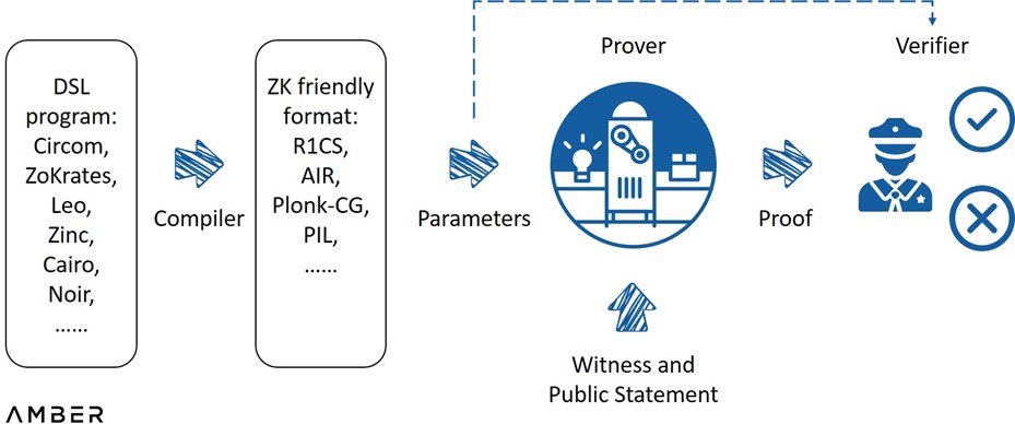
Source: ZK Whiteboard Sessions - Module One, by Prof. Dan Boneh
Multiple excellent proving systems have been developed, such as Marlin, Plonky2, Halo2, etc. Different proving systems adopt different trade-offs among proof size, the length of verifier time, and the necessity of a trusted setup[1]. After several years of exploration, it is possible to have constant level proof size (a few hundred bytes) and verifier time (several milliseconds) no matter how complicated the statements are.
However, the complexity of proof generation is still almost linear to the arithmetic circuit size, which could be several hundred times larger than the original tasks. This is because the prover has to at least read and evaluate the circuit. It could take several seconds to minutes or even hours. High computation costs and long proof generation times have been, and are still expected to be, the main obstacles for mass adoption and the advance of ZK technology.
Hardware acceleration can be used to help solve this bottleneck. Via assigning multiple tasks to most well suited hardware, it is a mutual supplement with algorithm or software optimization.
This report aims to help understand the market landscape, how it differs from previous mining markets, and potential opportunities. The report consists of three parts:
- Use cases from different projects and emerging trends.
- Solutions based on GPU, FPGA, and ASIC acceleration designs.
- Closing Thoughts
2. Use Cases
Mapping out use cases for ZK will help illustrate how the market is evolving. Different categories have different requirements, which will dynamically interact with hardware solutions’ supply. At the end of this section, we also show a brief comparison between ZKP and PoW (especially for Bitcoin).
2.1 Emerging Chains and Their Differentiated Requirements
Current demands for hardware acceleration are dominated by emerging chains using ZK technology, which can be broadly categorized into scaling solutions and privacy blockchains. ZK rollups or volitions execute transactions off the mainnet and submit a succinct validity proof via ‘call data’ function. Privacy blockchains use ZKPs to ensure transactions initiated by users are valid without publicly disclosing transaction details.
These blockchains use different proving systems to pick between the trade-offs among proof size, verifier time, trusted setups and others. For instance, a Plonk generated proof has constant-level small proof size (~400 Bytes) and verifier time (~6 ms), but will still need a universal trusted setup. In contrast, a Stark system doesn’t need a trusted setup but its proof size (~80 KB) and verifier time (~10ms) are larger and will increase with circuit size. Other systems have different tradeoffs. The upshot is that choices over these proving systems will lead to shifts of the “gravity center” of the computation load.
More specifically, nowadays a proving system can be generally described as PIOP (Polynomial Interactive Oracle Proof) + PCS (Polynomial Commitment Scheme). The former can be regarded as an agreed procedure for provers to persuade verifiers, and the latter mathematically ensures that the procedure cannot be compromised. As an analogy, PCS is the gun and PIOP is the bullet. Projects can modify PIOPs to cater their own needs and choose from different PCSs.
Georgios Konstantopoulos from Paradigm explains in his report on hardware acceleration that time used for proof generation is dominated by two types of computation tasks: MSM (multi-scalar multiplications) and FFT (Fast Fourier Transforms). However, instead of using a fixed number, establishing different PIOPs and choosing from different PCSs will bring different workload ratios of FFT / MSM. Using Stark as an extreme example, the PCS Stark uses, FRI (Fast Reed-Solomon Interactive Oracle Proofs of Proximity), is RS-code based instead of ecliptic curves used by KZG or IPA, so MSM is totally not involved in the whole proof generation. We show a rough order of the workload ratios for different proving systems as below, with the caveat that 1) It’s hard to estimate the exact ratio of the whole system; and 2) projects usually have their own modifications on the system when implementing.
Workload Ratios for Different Proving Systems[2]
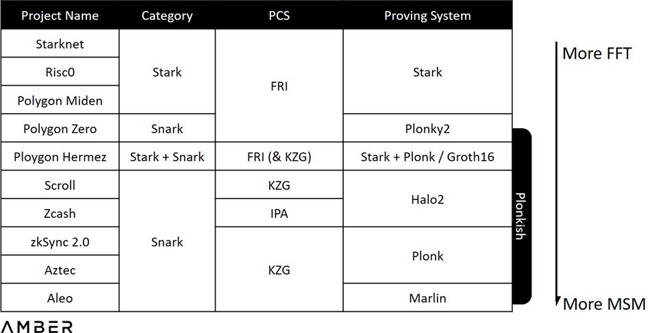
This will have a direct impact on the project’s preference of hardware types. Nowadays the most widely used hardware is GPU (Graphics Processing Unit) due to large supply and convenience for development. Additionally, parallelizing MSM calculation is quite convenient which suits GPU’s multi-core structure. However, as we will elaborate more on in the second section, FPGA (Field Programmable Gate Arrays) is possibly better at dealing with FFT. Projects who use Stark, such as Starknet and Hermez, could be more in need of FPGA than others.
Another takeaway from above is that this technology is still at an early stage, lacking standardized or dominant solutions. A full commitment to some algorithm-specific ASIC (Application-Specific Integrated Circuit) might be premature as well. As a result, developers are exploring a middle ground, which we’ll also explain more later.
2.2 Trend and New Paradigms
2.2.1 More Complicated Statements
Following the use cases we listed at the beginning, we should expect multiple purposes and more complicated proofs both for the crypto industry and the real world. Some of them don’t even have to comply with the present proving systems. Instead of following the usage of PIOP and PCS, they can develop new primitives that best suit their needs. In other areas such as MPC (multi-party computation), integrating ZK protocols into some parts of the work will largely improve its practicability. Ethereum is also recently planning on a KZG setup ceremony as part of the preparation work for Proto-Danksharding and further Danksharding in the future, dealing with data availability sampling. Even optimistic rollups could possibly adopt ZKP one day for better security and shorter disputing periods.
While many people may view ZK as an independent sector within the broader crypto industry, we believe that the proper mental model is to view ZK as a technology that can address multiple pain-points. In turn, more flexibility and generality for hardware acceleration will be needed to serve different systems and customers.
2.2.2 Locally Generated Proofs
ZKPs used for privacy instead of compressing information have notable structural differences. In order to hide transaction details, some random numbers will be involved during the proving process. Users will need to generate the proof locally, but most of them don’t have advanced hardware. What’s worse, if most dapps remain as web apps, proofs will need to be generated within browsers, which takes even longer. For example, when Manta started to build high-performance provers for WASM[3], they soon realized that “WASM gives users a 10x - 15x performance penalty compared with native speed”. To solve this, they have chosen to be a sponsor and architect for ZPrize, one of the largest ZKP acceleration competitions, and set up a particular track for acceleration for WASM. A client version is a much easier solution for these apps, but the downloading process will block out a non-trivial portion of potential users, and it doesn’t work with current extension wallets or other toolings either.
An alternative way is to partially outsource proof generation. Pratyush Mishra presented this approach during ZK Summit 7. Users first perform some lightweight computing, then give public statements and encrypted witness to several third parties, who take over and finish the rest of the proof. Following this approach, as long as one of those parties is honest, users’ privacy will not be leaked. It combines some toolings used by ZK protocols and MPC. Alternatively, users can trade bandwidth for computation: first generating a proof of large size, sending it to a third party who will compress it and post it on-chain.
Outsourcing Proof Generation
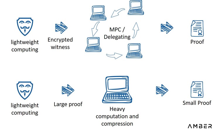
Source: Zero Knowledge Summit 7, by Pratyush Mishra from Aleo
2.3 Comparison with PoW Mining
Though it is natural to think of ZKP as a novel form of PoW, and accelerated hardware as a new kind of mining machine, ZKP generation is fundamentally different from PoW mining in terms of purpose and market structure.
2.3.1 Power Competition vs. Utility Computation
In order to gain block rewards and transaction fees, Bitcoin miners seek for a small enough hash via constantly iterating nonces, which are practically only relevant for reaching consensus. On the other hand, ZKP generation is a necessary procedure to fulfill practical utilities such as information compressing or privacy protection, but no longer necessarily responsible for consensus. Such differences will have impacts on the potential breadth of participation and reward distribution pattern. Below we list three existing designs of how miners will be coordinated for ZKP generation.
- Rates-are-Odds (Aleo): Aleo’s economic design is the closest to Bitcoin and other PoW protocols. Its consensus, PoSW (proof of succinct work), still requires miners to find a valid nonce, but the trial process is mainly dominated by repeatedly generating SNARK proofs that takes hashes of nonce and state root as part of the input, until the hash of some round’s proof itself is small enough. We call these PoW-alike mechanisms the Rates-are-Odds model because the number of trials you can process in a unit period roughly determines the probability you will gain the reward. In this model, miners stock large amounts of machines to gain better odds.
- Winner-Dominates (Polygon Hermez): Polygon Hermez adopts a simpler model. According to their public docs, two main characters participating are Sequencers, who collect all transactions and preprocess them as a new L2 batch, and Aggregators, who indicate their intentions of validation and compete to produce the proofs. For a given batch, the Aggregator that submits the first proof earns fees paid by the Sequencer. Without considering geographical distribution, network condition, and proving strategy, the Aggregator with the most advanced implementation and hardware will likely dominate.
- Party-Thresholds (Scroll): Scroll describes their design as ‘‘Layer2 proof outsourcing’’, where miners will be arbitrarily chosen to generate proofs after staking some amount of crypto. The one chosen needs to submit the proof within a set time period, otherwise its probability for next epochs will be adjusted downwards. A wrong proof will cause slashing. At first, Scroll will likely collaborate with a dozen miners for the stability or even run their own GPU cluster. As time goes by they plan to decentralize the whole process. We view the time limit as a parameter to adjust trade-offs between efficiency and decentralization. Starkware will likely also fall into this category. In the long run only those with machines that are able to accomplish proving in time can participate in proving.
These coordination designs have different trade-offs. We expect Aleo will have the most decentralized token distribution, Hermez to have the best efficiency, and Scroll with the lowest threshold to participate. But with accordance to the designs above, an arms race of zk hardwares may not be imminent.
2.3.2 Static vs. Evolving Algorithm
Another difference is that Bitcoin has a single, relatively static algorithm. Bitcoin core developers have always tried to comply with its initial design and spirit, to maintain network stability and avoid serious forks. Emerging chains or projects don’t have such legacy constraints, which gives them more flexibility to adjust their systems and algorithms.
We believe all these differences combined portray a more dispersed and dynamic market structure, compared with the simple and static PoW market. We suggest thinking of ZKP generations as a service (some start-ups name it ZK-as-a-Service), a means to an end, rather than an ultimate purpose in itself. This new paradigm will eventually form new business / revenue models which we will shed more light on in the last section. Before that, let’s first take a look at the multiple solutions.
3. Solutions
A CPU (central processing unit) is the main chip in a general computer, responsible for distributing instructions throughout the components on the motherboard. However, since a CPU is designed to handle a wide-range of tasks quickly, this versatility in turn limits its speed to deal with concurrency or some specific tasks, with GPU, FPGA, and ASIC commonly used as supplements. In this section we will focus on features, optimization process, current situation, and market for each of them.
3.1 GPU: Most Used Hardware at This Moment
GPU was initially designed for manipulating computer graphics and image processing, but its parallel structure makes it also a good choice for areas like computer vision, natural language processing, supercomputing, as well as PoW mining. Both MSM and FFT can be accelerated on GPU, especially for MSM via leveraging an algorithm called ‘pippenger’, and the development process is much simpler compared with FPGA or ASIC.
The idea for acceleration on GPU is quite straightforward: moving these computation concentrated tasks from CPU to GPU. Engineers will rewrite those parts into CUDA, a parallel computing platform and programming model developed by Nvidia for general computing on its own GPUs, or its competitor, OpenCL, launched by Apple and Khronos Group to provide a standard for heterogeneous computing so that users were no longer limited to Nvidia GPUs. These codes will then be compiled and run on the GPU directly. For more fine-grained acceleration, leaving aside algorithm improvement itself, developers can:
- Optimize memory by using as much fast memory and as little slow-access memory as possible in order to downscale the costly data transfer (especially for those between CPU and GPU).
- Optimize execution configuration by better balancing work across multiprocessors, building concurrent kernels, and allocating resources for tasks reasonably in order to lift hardware utilization, keeping them as busy as possible.
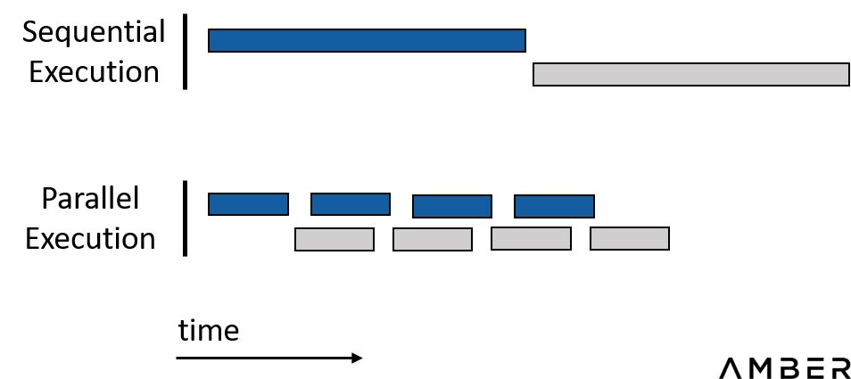
In short, try everything we can to parallelize the whole work process. Sequential execution, where different parts depend on each other’s results, should be avoided as much as possible.
Parrelization Saves Time
GPU Acceleration Design Flow

3.1.1 Large Developer Base and Convenience for Development
Unlike FPGA and ASIC, GPU development doesn’t involve hardware design. CUDA or OpenCL also have larger developer bases. Developers are able to start their own modification very quickly based on open source implementations. As an example, Filecoin published their first implementation for GPU back in 2020. Supranational also open sourced their general-purpose acceleration solution recently, which at this moment may be the best open source solution in class.
This advantage is even more obvious when taking into consideration works besides MSM and FFT . It’s true that proof generation is dominated by these two problems, but other parts can still take up a ratio of ~20% (source: Sin7Y’s whitepaper), so purely accelerating MSM and FFT will have a limited effect on the final time consumption. Even if time on these two problems are compressed to instantaneous, total time spent will still be one fifth compared with initial. Moreover, since it’s an emerging and evolving space, it is difficult to anticipate how this ratio will change in the future. To accelerate these heterogeneous works, given FPGA will need reconfiguration and ASIC probably needs re-design and manufacturing, GPU is of much more convenience.
3.1.2 Excess GPUs
The GPU market is dominated by Nvidia. According to Jon Peddie Research, its market share by discrete GPU shipments in Q1, 2022 was 78%. Although the prices of many cards are still highly inflated compared to the MSRP (Manufacturer’s Suggested Retail Price), their availability is continuing to improve. During 2021, over 50m units of GPUs ($52 billion dollars worth) were shipped. To put that amount into perspective, that was almost 8.5x the amount of FPGAs sold during the same period.
GPU Chip Market Share
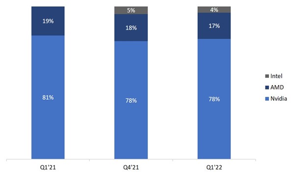
Source: Jon Peddie Research
For mining specifically, our conservative estimate is that approximately 6.26M GPUs will be freed from Ethereum PoW mining after Ethereum’s merge. We arrive at this number by multiplying Ethereum’s current hash rate (890 Th/s) by 90%, assuming that GPUs make up the vast majority of Ethereum’s hash rate. The resulting number (801 Th/s) is divided by the mining capacity (128 Mh/s) of the most advanced GPU card, the RTX 3090 Ti. This leads us to our conservative estimate of 6.26M GPUs. With ASIC dominating Bitcoin mining, no other projects using PoW can accommodate this bulk of mining power. Besides mining Ethereum forks or providing cloud services, pivoting to ZKP services is another choice that deserves exploring.
Ethereum Hash Rate

Source: Messari
3.2 FPGA: Balancing Cost & Effectiveness
FPGAs are integrated circuits with a programmable hardware fabric. The circuitry inside an FPGA chip is not hard etched thus it can be reconfigured multiple times by the designer adaptive to specific needs. On one hand, this effectively cuts off the huge manufacturing cost of an ASIC. On the other hand, more flexibility of usage of hardware resources than GPU reserves the potential of further acceleration and electricity saving. For instance, though optimizing FFT on GPU is still achievable, frequent shuffling of data will lead to large communication overhead between GPU and CPU. However, the shuffling is actually not completely random, by implementing the intrinsic logic directly to the circuit design, we can expect an FPGA to perform the task faster.
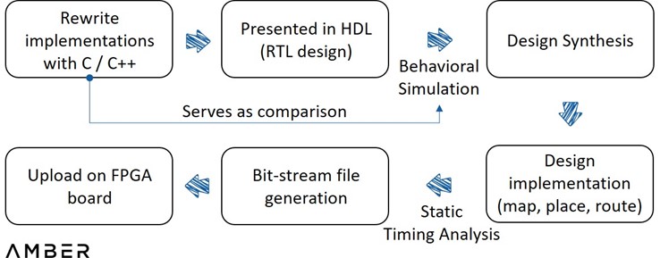
To achieve ZKP acceleration on an FPGA, a few steps are still required. First, a reference implementation for a particular proving system written in C / C++ is needed. Then, this implementation would need to be presented in HDL (Hardware Description Language) to describe the digital logic circuits at a high level.
Subsequently behavioral simulation would need to be performed to display the waveform of the inputs and outputs to see if the code ran as expected. This step is where the implementation is most involved. Engineers could compare the two outputs, instead of going through the whole process to identify some trivial bugs. Later on, synthesizer would translate HDL to the actual circuit design with elements such as gates and flip flops, followed by implementing the design to device architecture and more simulation analyses. Once proper operation of the circuits has been confirmed, a programming file will be finally created and loaded into an FPGA device.
FPGA Design Flow
3.2.1 Current Obstacles and Unestablished Infrastructure
Though some module optimization work on GPU can be reused, there are some new challenges:
- Due to higher level of memory safety and better cross-platform compatibility, open-source implementations for ZK are mostly written with Rust for a long time, but most FPGA development tools are adapted to C / C++, which hardware engineers are also more comfortable with. Teams might have to rewrite or translate those implementations before further actions.
- When writing those implementations, software engineers will be limited to a narrow scope of open-source libraries for C / C++ that can be mapped into hardware architecture by present development support.
- Besides those can be done relatively independently by software engineers and hardware engineers, some in-depth optimizations will rely on their close collaborations. For example, some modifications on algorithms will function equivalently as before, while saving a lot of hardware resources, but this can only be based on understanding of both components.
In short, unlike AI or other well-established areas, engineers will have to learn and nearly build from scratch for ZKP acceleration. Fortunately, we are seeing more progress. For example, Ingonyama proposed PipeMSM in their recent paper, an acceleration method for MSM on FPGA or ASIC.
3.2.2 A Duopoly Market
The FPGA market is a typical duopoly market. According to Frost & Sullivan, in 2019, Xilinx (acquired by AMD in February 2022) and Altera (acquired by Intel in December 2015) contribute ~85% of the global FPGA market by shipments. Early access to the most advanced FPGAs might demand close relationships with Intel or AMD. Additionally, this emerging space has already caught the attention of these industry behemoths. AMD is one of the technology providers for ZPrize.
The FPGA is a Typical Duopoly Market
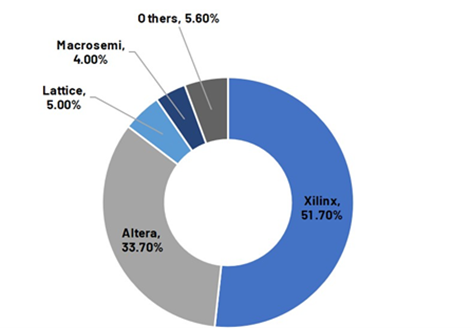
Source: Frost & Sullivan
Engineers already realized that one single FPGA doesn’t provide enough hardware resources for a complex ZKP generation, so they’ll have to use several bundled cards together for trials. Even after they complete their design, present standard FPGA cloud services offered by AWS and other cloud providers won’t serve them well. In addition, startups tackling acceleration solutions are usually too small to let AWS or others to host their customized hardware, and they don’t have enough resources to run their own servers either. Better alternatives might be collaborating with large miners or some Web3 native cloud providers. However, this relationship could be subtle considering in-house engineers of these mining firms will likely develop their own acceleration solutions at the same time.
3.3 ASIC: The Ultimate Weapon
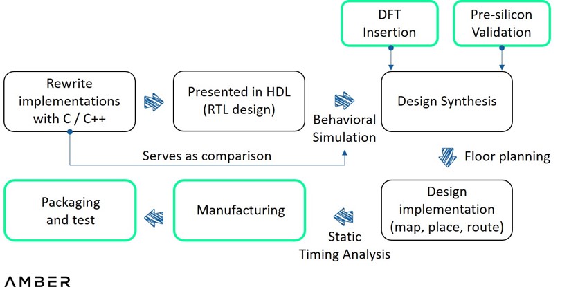
An ASIC is an integrated circuit (IC) chip customized for a particular use. Typically engineers still use HDL to specify the logic function of an ASIC in a similar way as in the case of FPGAs, but the resultant circuit is eventually drawn into silicon permanently, whereas in FPGAs the circuit is made by connecting thousands of configurable blocks. Unlike purchasing from Nvidia, Intel, or AMD, firms have to manage to host the whole process themselves, from circuit design all the way to fabrication and testing. An ASIC will be limited to some specific function, but inversely it enables designers with maximum freedom for resources allocation and circuit design, and thus large potential for performance and energy efficiency. Designers can eliminate wasted space, power and functionality, having the exact number of gates needed, or adjusting different blocks’ size best adapted to the intended application, etc.
In terms of the design flow, compared with FPGA, ASIC involves detailed pre-silicon verification (as well as DFT[4]) between HDL writing and synthesis, and floor plan before implementation. The former is for engineers to test the design in a virtual environment with sophisticated simulation and emulation tools, and the latter is to determine the size, shape, and locations of modules in a chip. After implementation of the design, all the files are sent to foundries such as TSMC or Samsung for test tape-out. If that succeeds, the prototype is then sent for assembly and test.
ASIC Design Flow
3.3.1 Relatively Generalized ASIC for ZK
A common critique for ASIC is that once the algorithm is changed, the previous chips will be totally useless, but it’s not necessarily the case.
Coincidentally, all those companies we talked with that are having a plan for ASIC are not betting on a specific proving system or project. Alternatively, they prefer to develop some programmable modules on top of the ASIC, so that different proving systems can be dealt with through these modules and only MSM and FFT tasks are assigned to ASIC. This will inevitably be suboptimal to a specific chip when used for a particular project, but sacrificing performance for better generality could be better than task-specific designs in near term.
3.3.1 Costly but Non-recurring Input
Not only is the design process of ASIC much more complicated than FPGA, but the manufacturing process consumes much more time and capital as well. Startups can directly reach out to foundries for tape-out or through some distributors. Not until waiting in line for around three months or longer, could they actually execute it. Mask and wafer constitute the main cost of tape-out. Masks are used to produce the pattern on the wafer, a thin slice of silicon. Startups usually choose MPW (multi-project wafer) arrangements that allow them to share mask and wafer fabrication cost with several other projects. However, the conservative estimate of a tape-out will still be as high as a few million dollars, depending on the process and amounts of chips they choose. Tape-out, along with assembly and test, will take another few months. If that works, they will finally get started preparing for mass production. However, if anything goes wrong, debug and failure analysis will take an unexpectable length of time, and another tape-out will be needed. It will take a few dozens of millions and around 18 months from initial design to mass production. Mitigant is that a large portion of the cost mentioned above is non-recurring. Moreover, the performance ASIC provides and energy and space it saves are usually significant, and the price could be relatively low.
4. Closing Thoughts
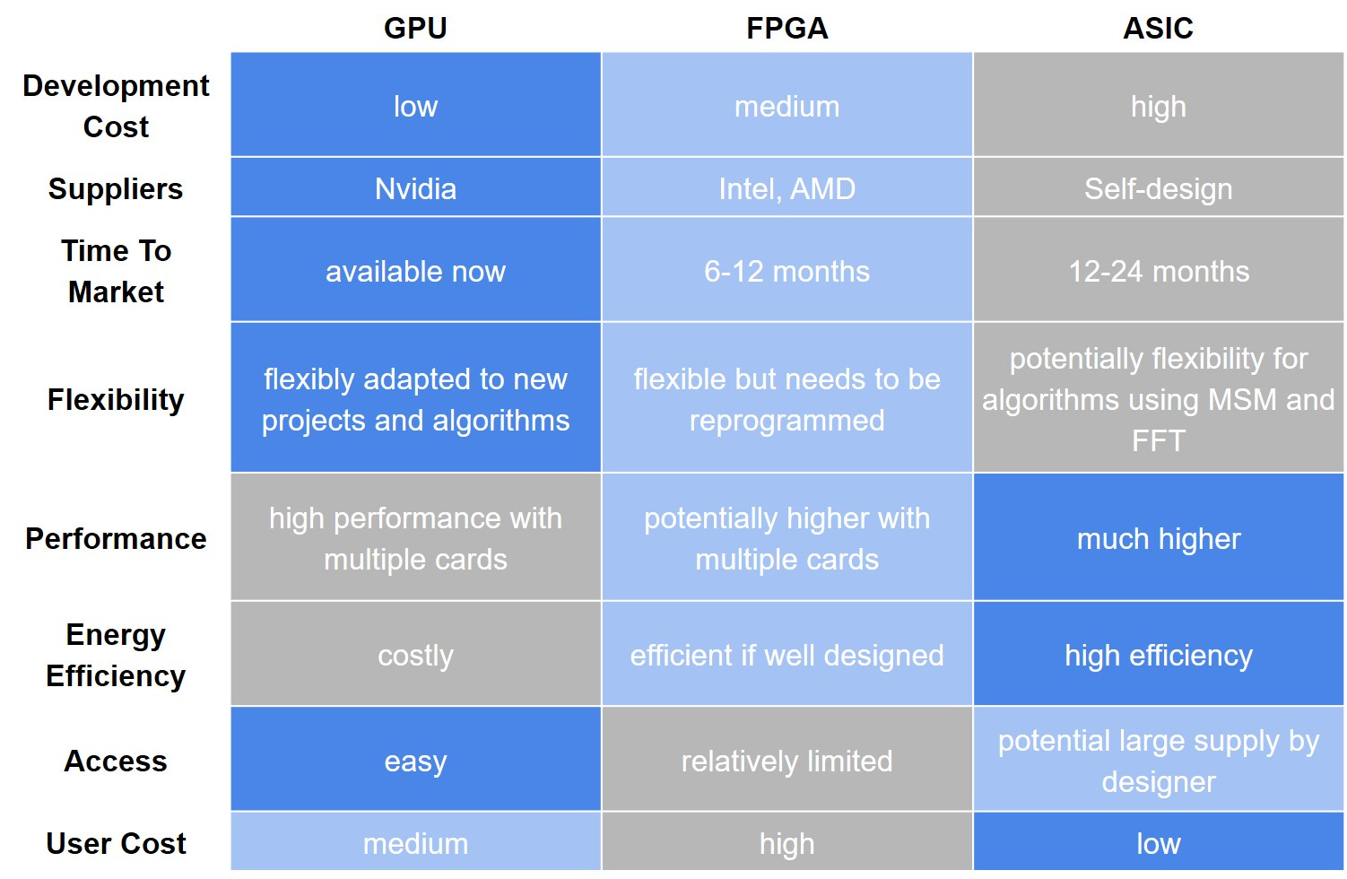
A general assessment of different hardware solutions is shown below.
Comparison of GPU, FPGA, and ASIC
Source: Amber
For a clearer perspective on possible business models, we show all potential market participants in one chart. Since interactions between them could be mixed and complicated, we categorize them simply by functionality.
Functionality Layers for Hardware Acceleration
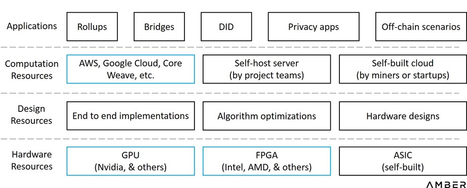
Except for developing a new GPU or FPGA chip, startups will be able to cut into this space from nearly any layer. They could choose to design and manufacture ASICs from scratch, packaging the chips into dedicated devices and sell them to miners, or they could sell bare chips to be assembled by downstream suppliers. They could also build their own servers, participating in proof generation or providing cloud services. Alternatively, they could choose to serve as a consultant company, providing design solutions but hands off actual operation. If they have robust partnerships or sufficient resources to cover across the value chain, they can also provide full-stack solutions to zk-applications, from hardware resources all the way to customized system designs.
Mass adoption for ZK is yet to happen, but building acceleration solutions is also a long-term process. We anticipate a tipping point. For builders and investors, the key question is when, not if.
Acknowledgments
Special thanks to Weikeng Chen (DZK), Ye Zhang (Scroll), Kelly (Supranational), and Omer (Ingonyama) for helping us understand all these details. Also thanks to Kai (ZKMatrix), Slobodan (Ponos), Elias and Chris (Inaccel), Heqing Hong (Accseal), and many others for offering their insight into the research.
A trusted setup ceremony is a procedure in which one or more parties jointly generate some data (parameters) that will be used later for running the proving system. These parties are expected to permanently delete or forget their respective secret used during the procedure (hence, ‘trust’) so that the protocol will not be compromised. ↑
Noting that technically Snark and Stark are not comparable concepts. Snark refers to a class of proving systems that satisfy some particular features, while Stark usually refers to the proving system initially developed by Starware in 2018. ↑
WebAssembly, a binary instruction format and virtual machine that brings near-native performance to web browser applications. ↑
Design for test, adding testability features to the design. ↑
Disclaimer: The information contained in this post (the “Information”) has been prepared solely for informational purposes, is in summary form, and does not purport to be complete. The Information is not, and is not intended to be, an offer to sell, or a solicitation of an offer to purchase, any securities. The Information does not provide and should not be treated as giving investment advice. The Information does not take into account specific investment objectives, financial situation or the particular needs of any prospective investor. No representation or warranty is made, expressed or implied, with respect to the fairness, correctness, accuracy, reasonableness or completeness of the Information. We do not undertake to update the Information. It should not be regarded by prospective investors as a substitute for the exercise of their own judgment or research. Prospective investors should consult with their own legal, regulatory, tax, business, investment, financial and accounting advisers to the extent that they deem it necessary, and make any investment decisions based upon their own judgment and advice from such advisers as they deem necessary and not upon any view expressed herein.